
Patterned silicon wafers, with their intricate surface designs and tailored properties, have revolutionized various fields of technology. These wafers, made from the same material that powers our beloved electronic devices, are no longer limited to the realm of microelectronics. With advancements in fabrication techniques and innovative applications emerging, patterned silicon wafers have become invaluable in optoelectronics, photovoltaics, biomedical research, MEMS devices, and even nanotechnology. In this blog post, we will delve into the significance of patterned silicon wafers, explore their traditional applications, discuss recent advancements, and uncover exciting prospects.
Table of Contents
Overview and Significance
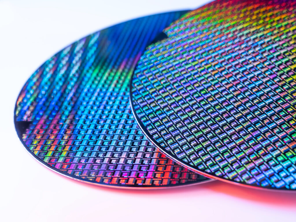
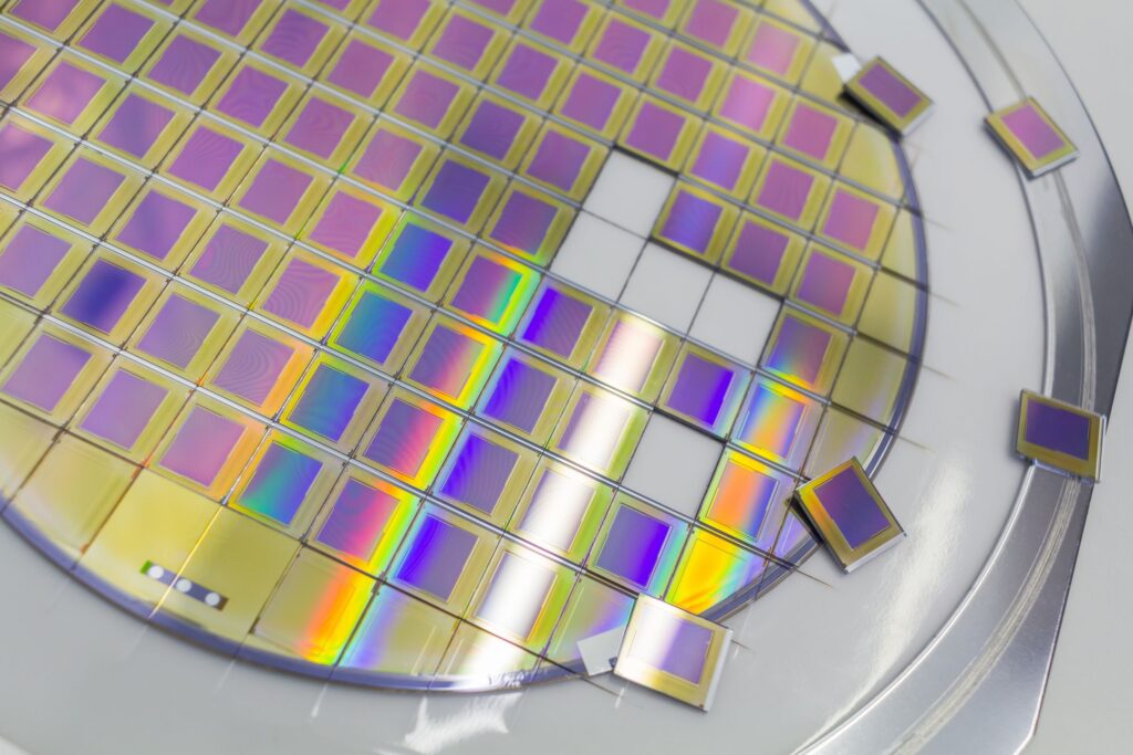
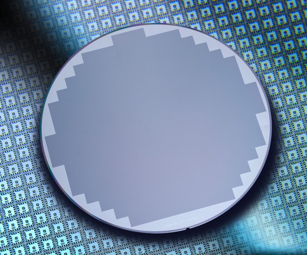
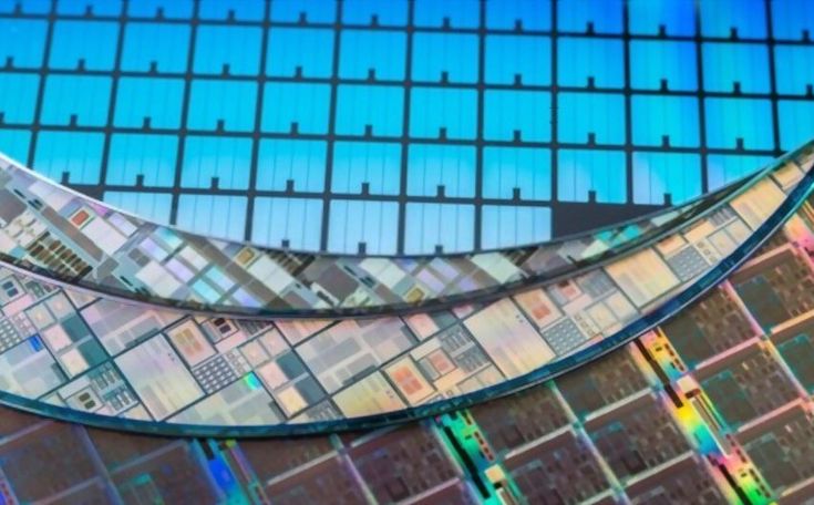
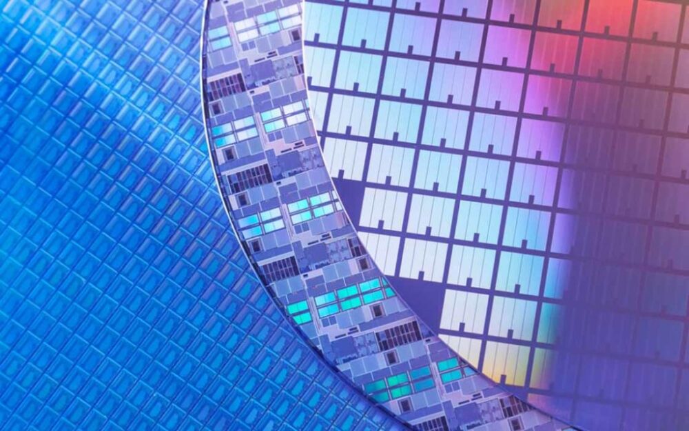
Patterned silicon wafers, as the name suggests, are silicon substrates with specific patterns etched onto their surfaces. These patterns can range from simple geometrical shapes to intricate microstructures, enabling enhanced functionality and performance in various applications. The ability to control the surface morphology and structure of silicon wafers has opened up new avenues for research and development, fostering breakthroughs in multiple industries. By harnessing the properties of silicon and manipulating its surface features, scientists and engineers have unlocked a plethora of applications that go far beyond traditional microelectronics.
Traditional Applications of Patterned Silicon Wafers in Microelectronics
Microelectronics has been the primary domain, fueling the development of smaller, faster, and more efficient electronic devices. By incorporating practices such as trenches, wells, and transistors on silicon wafers, the circuitry can be etched and created with precision. These wafers serve as the backbone of integrated circuits, microprocessors, and memory chips, powering our smartphones, computers, and countless other electronic gadgets. The uniformity and reliability have made them indispensable in the semiconductor industry, enabling the continued advancement of computing technology.
Advancements in Fabrication Techniques
Over the years, significant advancements have been made in patterned silicon wafer fabrication techniques, enabling the creation of more complex and intricate structures. Photolithography, ion implantation, and chemical etching are some of the key techniques employed in the manufacturing process. Additionally, innovative methods such as nanoimprint lithography and directed self-assembly have emerged, allowing for precise control over nanoscale designs. These advancements have not only improved the quality and resolution but also made them more cost-effective, paving the way for their adoption in a wider range of applications.
Emerging Applications in Optoelectronics
Textured semiconductor wafers have found interesting new uses in optoelectronics, which harnesses the interaction of light and electricity for a variety of functions. Scientists can manipulate the reflection, refraction, and absorption of light by modifying their surface designs, allowing the development of new optical equipment. Photonic integrated circuits, optical sensors, and displays with improved performance and efficiency are among these devices. They have the potential to completely transform industries like telecommunications, data communication, and display technology, ushering in a new era of high-speed, low-energy optical devices.
Enhanced Solar Cell Efficiency
Solar energy has emerged as a crucial alternative to fossil fuels, and patterned silicon wafers are playing a significant role in boosting the efficiency of solar cells. By texturing the surface, scientists can minimize reflection and increase light absorption, maximizing the conversion of sunlight into electricity. These textured wafers also reduce the amount of material required, making solar cells more cost-effective. Furthermore, they enable the integration of additional features such as antireflection coatings and passivation layers, further enhancing solar cell performance.
Biosensors and Drug Delivery
The biomedical field has embraced patterned silicon wafers for their ability to enable advanced biosensors and targeted drug delivery systems. By shaping the surface of silicon wafers with specific biomolecules or microstructures, researchers can create highly sensitive biosensors capable of detecting diseases at an early stage. These biosensors have applications in medical diagnostics, environmental monitoring, and food safety. Additionally, they can be used as a platform for controlled drug delivery, where drugs are loaded onto the surface and released in a controlled manner, improving therapeutic efficacy and reducing side effects.
Miniaturized Sensors and Actuators
Micro-electromechanical systems (MEMS) devices, which integrate mechanical elements, sensors, actuators, and electronics on a single chip, heavily rely on them. The precise patterning and etching techniques used in their fabrication allow for the creation of miniaturized sensors and actuators with high sensitivity and reliability. These MEMS devices find applications in a wide range of industries, including automotive, aerospace, healthcare, and consumer electronics. From pressure sensors to accelerometers and microfluidic devices, they have enabled the development of compact and efficient MEMS devices that have revolutionized multiple sectors.
Enabling Novel Nanostructures
Nanotechnology, the science, and engineering of manipulating matter at the nanoscale, has been greatly influenced by them. By leveraging advanced fabrication techniques, scientists can create nanoscale designs on silicon wafers, opening up possibilities for the synthesis of novel nanostructures. They serve as templates for the growth of nanowires, nanotubes, and other nano-scale materials with unique properties. These nanostructures have applications in fields such as energy storage, catalysis, and sensing.
Challenges and Solutions in Manufacturing
While patterned silicon wafers offer tremendous potential, their manufacturing process presents several challenges. Achieving high resolution, uniformity, and reproducibility in the patterning process is critical for their successful implementation. Additionally, scaling up production while maintaining cost-effectiveness is a challenge that needs to be addressed. Researchers and engineers are continuously working on developing advanced lithography techniques, materials, and process optimizations to overcome these challenges.
Future Prospects and Trends in Patterned Silicon Wafer Technology
The future of this technology is incredibly promising. As fabrication techniques continue to evolve, we can expect even more precise and intricate patterns on silicon wafers. The integration of multiple functionalities on a single wafer, such as combining electronics with optics or sensors, will drive the development of highly advanced and compact devices. Moreover, the utilization of novel materials, such as silicon photonics and flexible substrates, will expand the scope. The ongoing convergence of various disciplines and the emergence of new technologies will shape the future of these applications in ways we can only begin to imagine.
Conclusion: Unlocking the Full Potential
Patterned silicon wafers has come a long way since their inception in the world of microelectronics. From powering our electronic devices to revolutionizing optoelectronics, photovoltaics, biomedical research, MEMS devices, and nanotechnology, their impact is far-reaching. As fabrication techniques advance and new applications emerge, patterned silicon wafers will continue to push the boundaries of technological innovation. However, addressing the manufacturing challenges and exploring new possibilities will be key to unlocking their full potential. With ongoing research and collaborative efforts, patterned silicon wafers are poised to play a pivotal role in shaping the future of technology, transforming industries, and improving our lives in remarkable ways.
")

")


